VRS Zero Crossing discrete detector interface |
|
|---|---|
|
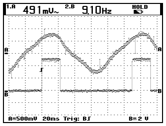
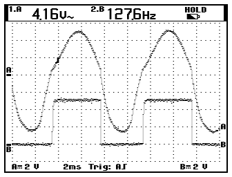
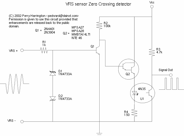
UPDATE 2012: This circuit doesn't actually detect Zero Crossing, it's more of a low level signal amplifier. I really just left this up here for people to tinker with. I would recommend looking at the LM1815 or LM139 datasheets. The LM1815 is a good one-stop solution, the LM139 datasheet has both single and double ended Zero Crossing detector example circuits. Be mindful of noise immunity, since example circircuits may not be very good at filtering noise. This circuit was born out of much tinkering. I have gone through several revisions to get what you see here. The circuit has the minimum number of components that I could think of. I have experimented with different components and values for every part shown in the schematic, these are the best component values that I could put together. For the true electronic purists, you will note that this circuit isn't a true zero crossing detector. It approximates a zero crossing detector. This circuit is tuned to only emit a pulse for the positive Zero Crossing, thus making it more suitable for microprocessor interfacing. The circuit will trigger at about 500mv rms, which corresponds to about 1 rev/sec with Ford VSS sensors (8 pulses per rev). D1 and D2 act as an input clamp. R1 is a current limiting resistor. Q1 is the zero crossing detector. R2 is a pullup for Q1. A smaller value results in a lower amplitude pulse because Q1 cannot conduct enough to overcome the resistor. Q2 is a darlington transistor to bump the current up enough to trigger U1's diode. The only critical value for Q2 is a current gain of 10,000 minimum. The current conducted through Q2 is only about 25ma, so surface mount components work for this too. R4 is a current limiting resistor for U1's diode. The darlington emits about 25ma with the 150ohm resistor, suitable to ensure that U1's diode is well on. R3 is a pullup for the collector follower of U1. The circuit isn't a TRUE zero crossing detector, as the pulse width and leading edge vary with the input voltage. At normal values that you would use for automotive applications, the detector output pulse goes high at zero crossing and low at zero crossing. The frequency of the input and output waveforms is the same, there is just a little drift at low input voltages. You can see the drift in the waveform below. The phase difference is about 35 degrees at the low end, and less than 10 degrees at higher input voltages (see second screen).
Here is a parts list:
 GIF Below are 2 scope captures of the circuit with a minimum input (8-10Hz) and a high frequency input. At very low input voltages the output pulse tends to shift the rising edge of the waveform. At higher voltages the pulse comes exactly at zero crossing.
High frequency conversion |